| CPC H01L 29/861 (2013.01) [H01L 29/2003 (2013.01)] | 13 Claims |
|
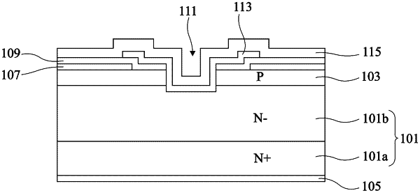
1. A semiconductor diode, comprising:
a first doped semiconductor region of a first conductivity type;
a second doped semiconductor region of a second conductivity type opposite to the first conductivity type, arranged on top of and in contact with an upper surface of the first semiconductor region;
a first conductive region arranged on top of and in direct contact with an upper surface of the second semiconductor region, the first conductive region comprising a through opening opposite a portion of the second semiconductor region;
a second conductive region made of a material different from that of the first conductive region, coating and in direct contact with the upper surface of the second semiconductor region opposite said opening;
a cavity extending through the second conductive region and through the second semiconductor region opposite a portion of said opening;
a dielectric region coating the lateral walls and a bottom of the cavity, the dielectric region disposed in direct contact with sides of the second doped semiconductor and with sides of the second conductive region on lateral walls of the cavity, and in direct contact with the first doped semiconductor region at the bottom of the cavity, the dielectric region overlapping the first conductive region and the second conductive region, the dielectric region overlapping the first conductive region and the second conductive region; and
a third conductive region coating the dielectric region on the lateral walls and at the bottom of the cavity, the third conductive region being further electrically in contact with the first conductive region and the second conductive region.
|