| CPC H01L 29/4234 (2013.01) [H01L 25/18 (2013.01); H01L 29/0649 (2013.01); H01L 29/401 (2013.01); H01L 29/66666 (2013.01); H01L 29/66833 (2013.01); H01L 29/7827 (2013.01); H01L 29/7926 (2013.01); H10B 12/05 (2023.02); H10B 12/31 (2023.02); H10B 12/50 (2023.02); H10B 43/27 (2023.02); H10B 43/35 (2023.02); H10B 43/40 (2023.02)] | 17 Claims |

|
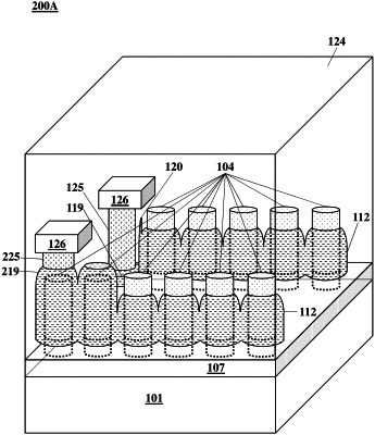
1. A modified vertical transistor comprising:
a semiconductor pillar standing over a substrate;
a gate dielectric disposed over at least a portion of said semiconductor pillar;
a gate surrounding a middle portion of said semiconductor pillar over said gate dielectric;
an extended gate region disposed over a top of said semiconductor pillar and extending upward from said gate;
and wherein said semiconductor pillar comprises:
a first region of a first doping type in said middle portion of said semiconductor pillar;
a second region of a second doping type occupying a top portion of said semiconductor pillar, extending partly into said middle portion from said top portion, and contiguous with said first region; and
a third region of said second doping type occupying a bottom portion of said semiconductor pillar, extending partly into said middle portion from said bottom portion, and contiguous with said first region.
|