| CPC H01L 29/205 (2013.01) [H01L 29/2003 (2013.01); H01L 29/207 (2013.01); H01L 33/325 (2013.01); H01S 5/3086 (2013.01); H01S 5/323 (2013.01)] | 12 Claims |
|
1. A semiconductor device comprising:
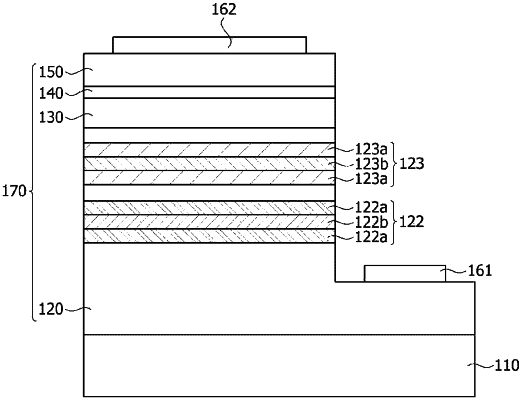
a semiconductor structure including a first conductive semiconductor layer, a second conductive semiconductor layer, and an active layer configured to emit light and disposed between the first conductive semiconductor layer and the second conductive semiconductor layer,
wherein the first conductive semiconductor layer includes a first superlattice layer including a plurality of first sub layers and a plurality of second sub layers, and individual first sublayer of the plurality of first sub layers and individual second sublayer of the plurality of second sub layers are alternately disposed,
wherein the first conductive semiconductor layer further includes a second superlattice layer disposed between the active layer and the first superlattice layer,
wherein the first sub layer includes a composition of indium,
wherein a maximum doping concentration of a first dopant in each of the plurality of first sub layers is different from a maximum doping concentration of the first dopant in each of the plurality of second sub layers, and a concentration of indium in each of the plurality of first sub layers is higher than a concentration of indium in each of the plurality of second sub layers,
wherein a concentration of indium in the active layer is higher than a concentration of indium in the second superlattice layer, and the concentration of indium in the second superlattice layer is higher than a concentration of indium in the first superlattice layer, and
wherein a portion of the first conductive semiconductor layer that is between the substrate and the first superlattice layer includes the highest doping concentration of the first dopant in the semiconductor device.
|