| CPC H01L 29/1075 (2013.01) [H01L 29/778 (2013.01); H01L 29/7786 (2013.01)] | 13 Claims |
|
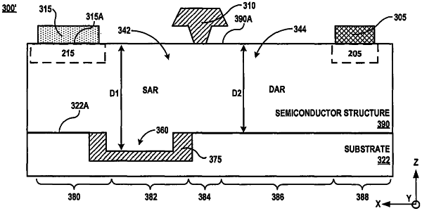
1. A semiconductor device comprising:
a substrate, wherein an upper surface of the substrate comprises a recess region;
a semiconductor structure on the substrate, a portion of the semiconductor structure within the recess region; and
a gate contact, a drain contact, and a source contact on the semiconductor structure,
wherein the recess region is in between the gate contact and the source contact and does not vertically overlap the drain contact,
wherein the semiconductor device comprises a high electron mobility transistor (HEMT) and the semiconductor structure comprises a channel layer and a barrier layer on the channel layer, and the channel layer extends continuously from underneath the source contact to underneath the drain contact,
wherein the portion of the semiconductor structure that is within the recess region is an undoped Group III-nitride layer, and
wherein the substrate comprises an n-type semiconductor substrate that includes a p-type impurity region adjacent the recess region.
|