| CPC H01L 25/0657 (2013.01) [H01L 23/3171 (2013.01); H01L 23/49816 (2013.01); H01L 23/49827 (2013.01); H01L 23/49861 (2013.01); H01L 24/05 (2013.01); H01L 24/12 (2013.01); H01L 2224/02372 (2013.01); H01L 2224/13111 (2013.01)] | 16 Claims |
|
1. A semiconductor package comprising:
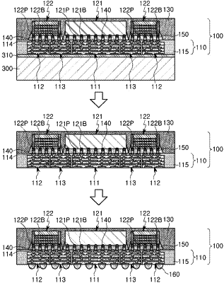
an interposer including a first connection structure having a first redistribution conductor, a plurality of second connection structures each having a second redistribution conductor and disposed around the first connection structure, a plurality of third connection structures each having a third redistribution conductor and disposed between the first connection structure and the plurality of second connection structures, and a passivation layer filling spaces between the first connection structure, the plurality of second connection structures, and the plurality of third connection structures;
a first semiconductor chip disposed on the interposer to overlap the first connection structure and at least a portion of the plurality of third connection structures, in a stacking direction of the first semiconductor chip on the interposer;
a second semiconductor chip disposed on the interposer to overlap at least a portion of the plurality of second connection structures and at least a portion of the plurality of third connection structures, in a stacking direction of the second semiconductor chip on the interposer; and
a plurality of electrical connection structures disposed below the interposer, and electrically connected to the first semiconductor chip and the second semiconductor chip,
wherein the first redistribution conductor electrically connects the first semiconductor chip to at least a portion of the plurality of electrical connection structures,
the second redistribution conductor electrically connects the second semiconductor chip to at least a portion of the plurality of electrical connection structures, and
the third redistribution conductor electrically connects the first semiconductor chip and the second semiconductor chip to each other,
wherein each of the first connection structure, the plurality of second connection structures, and the plurality of third connection structures further includes a plurality of insulation layers,
wherein each of the first redistribution conductor, the second redistribution conductor, and the third redistribution conductor includes a plurality of redistribution layers disposed in or on the plurality of insulation layers, and a plurality of connection vias penetrating each of the plurality of insulation layers and electrically connecting the plurality of redistribution layers to each other,
wherein the passivation layer and each of the plurality of insulation layers includes a photosensitive insulation layer,
wherein each of the plurality of insulation layers is a positive-type photosensitive insulation layer, and
wherein the passivation layer is a negative-type photosensitive insulation layer.
|