| CPC H01L 23/5386 (2013.01) [H01L 21/4853 (2013.01); H01L 21/4857 (2013.01); H01L 23/00 (2013.01); H01L 23/3121 (2013.01); H01L 23/49822 (2013.01); H01L 23/49838 (2013.01); H01L 23/49894 (2013.01); H01L 23/5383 (2013.01); H01L 24/14 (2013.01); H01L 24/16 (2013.01); H01L 24/17 (2013.01); H01L 24/73 (2013.01); H01L 24/97 (2013.01); H01L 25/0652 (2013.01); H01L 25/0655 (2013.01); H01L 25/18 (2013.01); H01L 25/50 (2013.01); H01L 21/561 (2013.01); H01L 21/568 (2013.01); H01L 23/5384 (2013.01); H01L 24/13 (2013.01); H01L 2224/1403 (2013.01); H01L 2224/14132 (2013.01); H01L 2224/16145 (2013.01); H01L 2224/16225 (2013.01); H01L 2224/16227 (2013.01); H01L 2224/1703 (2013.01); H01L 2224/17181 (2013.01); H01L 2224/73204 (2013.01); H01L 2224/81005 (2013.01); H01L 2224/95001 (2013.01); H01L 2224/97 (2013.01); H01L 2924/1517 (2013.01); H01L 2924/15192 (2013.01); H01L 2924/15311 (2013.01); H01L 2924/381 (2013.01)] | 20 Claims |
|
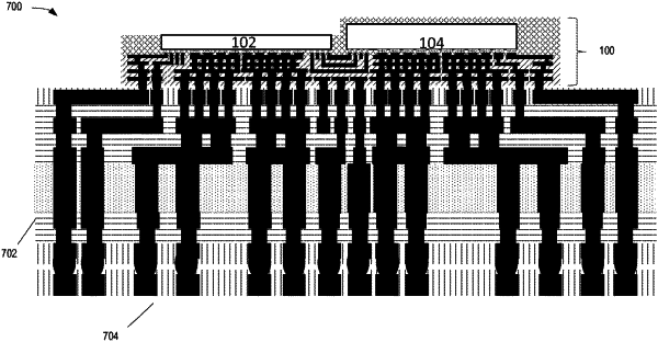
1. A system, comprising:
a multi-chip package, comprising:
a substrate having a top side opposite a bottom side, the substrate having a lateral width;
a first die coupled to the top side of the substrate by a first plurality of contacts;
a second die coupled to the top side of the substrate by a second plurality of contacts, the second die laterally spaced apart from the first die, and the second die having a thickness different than a thickness of the first die;
a first plurality of interconnects in the substrate, the first plurality of interconnects comprising horizontal portions and vertical portions;
a second plurality of interconnects in the substrate, the second plurality of interconnects comprising a first interconnect in a first sub-surface layer of the substrate and coupling an outermost contact of the first plurality of contacts to an outermost contact of the second plurality of contacts, and the second plurality of interconnects comprising a second interconnect in a second sub-surface layer of the substrate, the second sub-surface layer beneath the first sub-surface layer, and the second interconnect coupling a next outermost contact of the first plurality of contacts to a next outermost contact of the second plurality of contacts; and
a mold compound laterally adjacent to and between the first die and the second die;
an interposer having a top side opposite a bottom side, wherein the bottom side of the substrate of the multi-chip package is coupled to the top side of the interposer, and wherein the interposer has a lateral width greater than the lateral width of the substrate; and
a printed circuit board having a top side opposite a bottom side, wherein the bottom side of the interposer is coupled to the top side of the printed circuit board.
|