| CPC H01L 23/5283 (2013.01) [H01L 21/76816 (2013.01); H01L 21/76829 (2013.01); H01L 21/76846 (2013.01); H01L 21/76877 (2013.01); H01L 21/76885 (2013.01); H01L 21/76897 (2013.01); H01L 23/5221 (2013.01); H01L 23/5226 (2013.01); H01L 23/53209 (2013.01); H01L 23/53228 (2013.01); H01L 23/53238 (2013.01); H01L 23/53252 (2013.01); H01L 23/53266 (2013.01); H01L 23/53295 (2013.01); H01L 21/76834 (2013.01)] | 22 Claims |
|
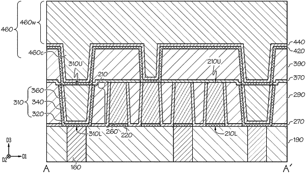
1. A method of forming an integrated circuit device, the method comprising:
forming a first metal wire on a first insulating layer, the first metal wire comprising a first lower surface that faces the first insulating layer;
after the first metal wire is formed, forming a lower etch stop layer on the first metal wire and the first insulating layer;
forming a second insulating layer on the lower etch stop layer, wherein the first metal wire is provided in the second insulating layer;
forming an opening extending through the second insulating layer and the lower etch stop layer;
forming a second metal wire in the opening, the second metal wire comprising a second lower surface that faces the first insulating layer and is coplanar with the first lower surface;
removing a portion of the second insulating layer and a portion of the lower etch stop layer to expose an upper surface of the first metal wire;
forming an upper etch stop layer on the first metal wire, the second metal wire, and the second insulating layer;
forming a third insulating layer on the first metal wire, the second metal wire, and the upper etch stop layer; and
forming an upper wire on the first metal wire, the second metal wire, and the third insulating layer.
|
|
18. A method of forming an integrated circuit device, the method comprising:
forming a first metal wire on a first insulating layer;
after the first metal wire is formed, forming a lower etch stop layer on the first metal wire and the first insulating layer;
forming a second insulating layer on the lower etch stop layer, wherein the first metal wire is in the second insulating layer;
forming an opening extending through the second insulating layer and the lower etch stop layer to expose a portion of an uppermost surface of the first insulating layer; and
forming a second metal wire in the opening, on the exposed portion of the uppermost surface of the first insulating layer;
wherein a lower surface of the second metal wire is coplanar with a lower surface of the first metal wire; and
wherein said forming a second metal wire in the opening comprises recessing an upper surface of the second metal wire toward the first insulating layer relative to an upper surface of the first metal wire.
|
|
22. A method of forming an integrated circuit device, the method comprising:
forming a first metal wire on a first insulating layer;
after the first metal wire is formed, forming a lower etch stop layer on the first metal wire and the first insulating layer;
forming a second insulating layer on the lower etch stop layer, wherein the first metal wire is in the second insulating layer;
forming an opening extending through the second insulating layer and the lower etch stop layer;
forming a second metal wire in the opening, wherein a lower surface of the second metal wire is coplanar with a lower surface of the first metal wire;
removing a portion of the second insulating layer and a portion of the lower etch stop layer to expose an upper surface of the first metal wire; and
forming an upper etch stop layer on the exposed upper surface of the first metal wire, and on the second metal wire and the second insulating layer.
|