| CPC H01L 21/7682 (2013.01) [H01L 21/76807 (2013.01); H01L 21/76808 (2013.01); H01L 21/76813 (2013.01); H01L 21/76828 (2013.01); H01L 21/76831 (2013.01); H01L 21/76897 (2013.01); H01L 23/5283 (2013.01)] | 20 Claims |
|
1. A method comprising:
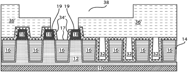
forming trenches within an insulating layer disposed over a semiconductor substrate;
filling the trenches with conductive material to form conductive regions;
selectively forming first dielectric regions on a pattern over exposed top surfaces of the insulating layer;
forming a mask over the semiconductor substrate and removing the first dielectric regions in areas not covered by the mask;
depositing an inter-layer dielectric over remaining first dielectric regions, the conductive regions, and the insulating layer; and
etching a portion of the inter-layer dielectric between two of the remaining first dielectric regions to form a self-aligned via.
|