| CPC G11C 29/42 (2013.01) [G06F 3/0611 (2013.01); G06F 3/064 (2013.01); G06F 3/0659 (2013.01); G06F 3/0679 (2013.01); G11C 29/40 (2013.01); G11C 29/44 (2013.01); G11C 29/765 (2013.01); G11C 2029/4002 (2013.01)] | 17 Claims |
|
1. A system comprising:
a memory device comprising a plurality of memory planes; and
a processing device, operatively coupled with the plurality of memory planes, wherein the processing device is configured to:
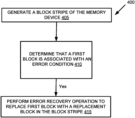
identify a first block residing on a memory plane of the memory device, wherein the first block is associated with an error condition by determining a failure of a memory access operation associated with the first block, and wherein the memory access operation comprises one of an erase operation, a program operation, or a read operation; and
responsive to identifying the first block, perform an error recovery operation to replace the first block with a second block by determining an address of the first block and storing the address in a data structure, wherein the second block resides on the memory plane.
|