| CPC G09G 3/3233 (2013.01) [G09G 2300/0852 (2013.01); G09G 2310/061 (2013.01); G09G 2320/0233 (2013.01)] | 3 Claims |
|
1. A method for driving a display panel, wherein
the display panel, comprising:
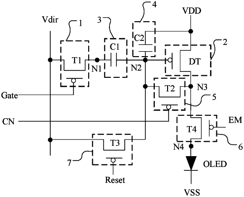
a pixel driving circuit, wherein the pixel driving circuit comprises:
a signal writing circuit connected to a composite signal end, a gate driving signal end, and a first node, and configured to transmit a signal of the composite signal end to the first node in response to a signal of the gate driving signal end;
a driving circuit connected to a first power supply end, a second node, and a third node, and configured to input a driving current to the third node according to a signal of the second node;
a first memory circuit connected between the first node and the second node;
a second memory circuit connected between the second node and the first power supply end;
a compensation circuit connected to the second node, the third node, and a control signal end, and configured to connect the second node and the third node in response to a signal of the control signal end;
a light-emitting control circuit connected to the third node, a fourth node, and an enable signal end, and configured to connect the third node and the fourth node in response to a signal of the enable signal end; and
a reset circuit connected to the composite signal end, the second node, and a reset signal end, and configured to transmit the signal of the composite signal end to the second node in response to a signal of the reset signal end, wherein the reset circuit is directly connected to the composite signal end;
wherein the composite signal end is configured to output an initialization signal in a reset phase, output a reference voltage signal in a threshold establishing phase, and output a data signal in a data writing phase, and wherein the initialization signal is different from the reference voltage signal; and
wherein the pixel driving circuit and other pixel driving circuits in a same row are connected to the same enable signal end; and
in a same frame, enable signal ends connected to pixel driving circuits in a plurality rows are configured to output active levels row by row, wherein a duration of an active level output by the enable signal end connected to each row of the pixel driving circuits is equal, and the duration of the active level output by the enable signal end connected to each row of the pixel driving circuits is less than a duration of a scanning period;
one frame period of the display panel comprises a first blank period, the scanning period, and a second blank period in order; and
the reset phase and the threshold establishing phase of each pixel driving circuit of the display panel are within a second blank period of a previous frame.
|