| CPC G06F 3/0448 (2019.05) [G06F 3/0446 (2019.05); G06F 2203/04102 (2013.01)] | 20 Claims |
|
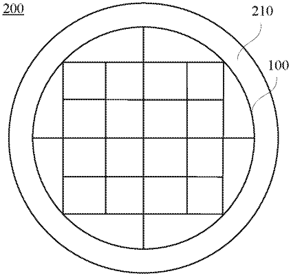
1. A touch structure, comprising:
a plurality of electrode plates, the plurality of electrode plates being located on a same virtual reference plane, and each electrode plate having a sensing surface; a smallest enclosed pattern region where a whole of the plurality of electrode plates is located being a touch region; wherein
the plurality of electrode plates include a plurality of first electrode plates, each first electrode plate has a designated edge, and the designated edge constitutes a part of a boundary of the touch region; at least one designated edge is arc-shaped; and
an area of a sensing surface of each first electrode plate is in a range of 10 mm2 to 35 mm2.
|