| CPC G01L 19/0092 (2013.01) [H03H 9/02015 (2013.01); H03H 9/02574 (2013.01); H03H 9/14502 (2013.01); G01N 29/022 (2013.01); G01N 2291/014 (2013.01)] | 13 Claims |
|
1. A method of measuring a plasma parameter in a plasma chamber, comprising:
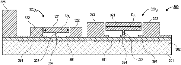
providing a diagnostic substrate in the plasma chamber, wherein the diagnostic substrate comprises a first resonator with a first geometry and a second resonator with a second geometry;
measuring a baseline response from the first resonator and the second resonator in a vacuum without a plasma;
striking the plasma in the plasma chamber, wherein the first resonator and the second resonator are within the plasma;
measuring a first resonance frequency of the first resonator and a second resonance frequency of the second resonator;
extracting the plasma parameter or a wafer parameter from the first resonance frequency and the second resonance frequency; and
measuring a resonator response of the first resonator and the second resonator to a varying bias applied to the first resonator and the second resonator by a first guard ring and a second guard ring.
|