US 11,889,772 B2
Methods for forming memory devices, and associated devices and systems
Michael B. Jeppson, Lehi, UT (US)
Assigned to Micron Technology, Inc., Boise, ID (US)
Filed by Micron Technology, Inc., Boise, ID (US)
Filed on Jun. 6, 2022, as Appl. No. 17/833,477.
Application 17/833,477 is a continuation of application No. 16/914,887, filed on Jun. 29, 2020, granted, now 11,398,599.
Prior Publication US 2022/0302387 A1, Sep. 22, 2022
This patent is subject to a terminal disclaimer.
Int. Cl. H10N 70/00 (2023.01); H10B 63/00 (2023.01); H10N 70/20 (2023.01)
CPC H10N 70/063 (2023.02) [H10B 63/24 (2023.02); H10B 63/80 (2023.02); H10N 70/231 (2023.02); H10N 70/882 (2023.02)] 19 Claims
OG exemplary drawing
 
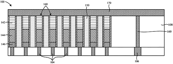
1. A method of manufacturing a memory device, the method comprising:
forming a memory stack in a recess of an insulative material by—
forming a metallization layer in the recess;
depositing a selector layer in the recess over the metallization layer;
depositing a memory cell layer over the selector layer; and
etching the memory stack to define a plurality of memory elements.