| CPC H10K 59/131 (2023.02) [H10K 50/841 (2023.02); H10K 2102/00 (2023.02)] | 9 Claims |

|
1. A display device, comprising:
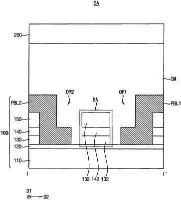
an array substrate including a pixel array disposed on a display area, a first transfer wiring disposed on a peripheral area adjacent to the display area and electrically connected to the pixel array, a second transfer wiring disposed on the peripheral area adjacent to the display area and electrically connected to the pixel array, and a barrier member disposed between the first transfer wiring and the second transfer wiring, the barrier member including an inorganic insulation material, wherein the first and second transfer wirings provide different power voltages from each other to the pixel array; and
a sealing member disposed between the array substrate and an encapsulation substrate to combine the array substrate with the encapsulation substrate, the sealing member contacting at least a portion of the first transfer wiring and the second transfer wiring, the sealing member including a glassy material and surrounding the display area in a plan view,
wherein the first transfer wiring and the second transfer wiring are spaced apart from the barrier member such that a first portion of the sealing member is disposed in a first recess between the first transfer wiring and a first side of the barrier member adjacent to the first transfer wiring and a second portion of the sealing member is disposed between the second transfer wiring and a second side of the barrier member adjacent to the second transfer wiring, and
wherein a first portion of the first transfer wiring is disposed in the first recess, and wherein a second portion of the first transfer wiring extends along a side surface and an upper surface of an insulating layer adjacent to the first recess, and contacts the sealing member.
|