US 11,889,723 B2
Display device including a light blocking layer over a pixel defining layer
Byung-chul Kim, Yongin-si (KR); Sujeong Kim, Yongin-si (KR); Kiyoung Yeon, Yongin-si (KR); Sun-kyu Joo, Yongin-si (KR); Chul Huh, Yongin-si (KR); Inok Kim, Yongin-si (KR); Hyeran Mun, Yongin-si (KR); Inseok Song, Yongin-si (KR); Wooyoung Lee, Yongin-si (KR); and Yui-ku Lee, Yongin-si (KR)
Assigned to Samsung Display Co., Ltd., Yongin-si (KR)
Filed by Samsung Display Co., Ltd., Yongin-si (KR)
Filed on Oct. 18, 2021, as Appl. No. 17/504,242.
Application 16/930,586 is a division of application No. 15/984,618, filed on May 21, 2018, granted, now 10,756,154, issued on Aug. 25, 2020.
Application 17/504,242 is a continuation of application No. 16/930,586, filed on Jul. 16, 2020, granted, now 11,158,699.
Claims priority of application No. 10-2017-0091659 (KR), filed on Jul. 19, 2017.
Prior Publication US 2022/0037443 A1, Feb. 3, 2022
Int. Cl. H10K 59/126 (2023.01); H10K 50/86 (2023.01); H10K 50/844 (2023.01); H10K 59/122 (2023.01); H10K 59/124 (2023.01); H10K 71/00 (2023.01); H01L 27/12 (2006.01); H10K 59/35 (2023.01); H10K 59/38 (2023.01); H10K 59/40 (2023.01); H10K 59/131 (2023.01); H10K 59/12 (2023.01); H10K 59/121 (2023.01)
CPC H10K 59/126 (2023.02) [H10K 50/844 (2023.02); H10K 50/86 (2023.02); H10K 50/865 (2023.02); H10K 59/122 (2023.02); H10K 59/124 (2023.02); H10K 71/00 (2023.02); H01L 27/124 (2013.01); H01L 27/1248 (2013.01); H10K 59/1201 (2023.02); H10K 59/1213 (2023.02); H10K 59/131 (2023.02); H10K 59/35 (2023.02); H10K 59/353 (2023.02); H10K 59/38 (2023.02); H10K 59/40 (2023.02)] 17 Claims
OG exemplary drawing
 
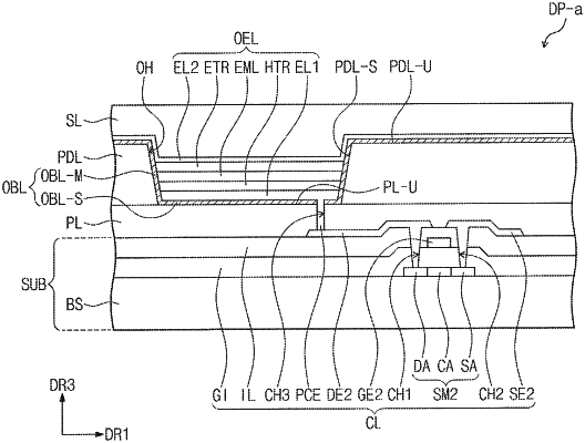
1. A display device, comprising:
a circuit layer;
an insulating layer on the circuit layer;
a pixel defining layer on the insulating layer, the pixel defining layer having an opening;
a first electrode on the insulating layer;
a light blocking layer including a first part that extends between the insulating layer and the first electrode in the opening;
at least one organic layer in the opening and on the first electrode;
a second electrode on the at least one organic layer and the pixel defining layer;
an encapsulating layer on the second electrode, and the encapsulating layer overlaps the at least one organic layer and the pixel defining layer;
an input sensor on the encapsulating layer; and
an optical member on the input sensor,
wherein the light blocking layer includes at least one light absorbent.