| CPC H10K 59/121 (2023.02) [H10K 50/844 (2023.02); H10K 59/1213 (2023.02); H10K 59/1216 (2023.02); H10K 59/65 (2023.02); H10K 71/00 (2023.02); G06F 3/044 (2013.01); G09G 3/3233 (2013.01); G09G 2300/0426 (2013.01); G09G 2300/0842 (2013.01); G09G 2360/14 (2013.01); H01L 27/127 (2013.01); H01L 27/1225 (2013.01); H01L 27/1251 (2013.01); H01L 27/1255 (2013.01); H01L 29/66757 (2013.01); H01L 29/66969 (2013.01); H01L 29/7869 (2013.01); H01L 29/78675 (2013.01); H10K 59/1201 (2023.02)] | 12 Claims |

|
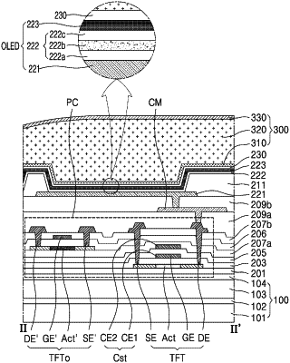
1. A display apparatus comprising:
a substrate comprising a transmission area having a first through hole, a display area surrounding the transmission area, and a middle area disposed between the transmission area and the display area;
a pixel circuit disposed on the display area, the pixel circuit comprising a first thin film transistor including a first semiconductor layer including polycrystalline silicon and a second thin film transistor including a second semiconductor layer including an oxide semiconductor;
a display element including a pixel electrode electrically connected to the pixel circuit, an opposite electrode disposed on the pixel electrode, and an intermediate layer disposed between the pixel electrode and the opposite electrode and including an emission layer; and
a groove disposed in the middle area while surrounding the first through hole,
wherein the groove comprises:
a first hole or a first recess disposed in a base layer of the substrate,
a second hole disposed in at least one inorganic insulating layer on the substrate and overlapping the first hole or the first recess in a plan view,
a pair of tips obtained by extending the at least one inorganic insulating layer toward a center of the second hole; and
a pair of pattern layers overlapping the pair of tips and including a material that is same as a material included in the first semiconductor layer or the second semiconductor layer.
|