| CPC H10K 50/856 (2023.02) [H10K 50/844 (2023.02); H10K 59/38 (2023.02); G02F 1/133509 (2013.01); G02F 1/133512 (2013.01); G02F 1/133514 (2013.01); G02F 1/136209 (2013.01); G09G 2300/0408 (2013.01); H10K 50/15 (2023.02); H10K 50/16 (2023.02); H10K 50/17 (2023.02); H10K 50/171 (2023.02); H10K 59/126 (2023.02); H10K 59/127 (2023.02)] | 20 Claims |

|
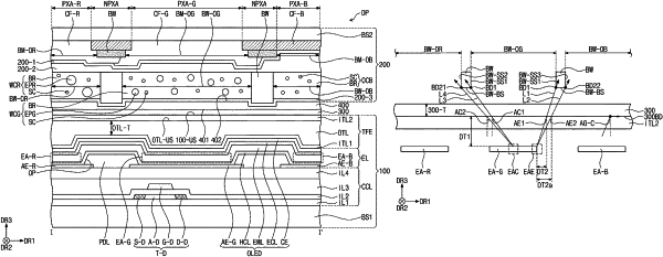
1. A display panel, comprising:
a first pixel area, a second pixel area, a third pixel area, and a peripheral area that is adjacent to the first, second and third pixel areas;
a base layer;
a circuit layer disposed on the base layer;
an emission layer disposed on the circuit layer and including a first emission area, a second emission area, and a third emission area, wherein each of the first, second and third emission areas generates source light, and wherein the first, second and third emission areas respectively correspond to the first pixel area, the second pixel area, and the third pixel area;
an organic encapsulation layer disposed on the emission layer, wherein a top surface of the organic encapsulation layer is flat;
an inorganic encapsulation layer disposed on the top surface of the organic encapsulation layer and having a first refractive index;
a functional layer disposed on the inorganic encapsulation layer and having a second refractive index less than the first refractive index; and
a partition wall disposed on the functional layer and including a first opening, a second opening, and a third opening, wherein the first, second and third openings respectively correspond to the first pixel area, the second pixel area, and the third pixel area,
wherein a total reflection critical angle between the inorganic encapsulation layer and the functional layer is less than a reference incident angle of reference light traveling from the first emission area toward the partition wall.
|