| CPC H10K 50/844 (2023.02) [H10K 71/00 (2023.02)] | 18 Claims |

|
1. A display substrate, comprising:
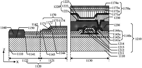
a base substrate comprising a display region and a peripheral region, wherein the peripheral region surrounds the display region, an edge of the peripheral region away from the display region is identical to an edge of the base substrate, the peripheral region comprises a first peripheral region and a second peripheral region, and the first peripheral region is between the display region and the second peripheral region;
a pixel drive layer on the display region of the base substrate;
a light-emitting device on the pixel drive layer;
an encapsulation layer on the light-emitting device, wherein an orthographic projection of the encapsulation layer on the base substrate covers the display region and the first peripheral region;
a first insulation layer on the base substrate, wherein the first insulation layer comprises a first notch in the second peripheral region at a position of at least a part of the edge of the base substrate, the first notch extends along the edge of the base substrate, and a side edge of the first notch away from the display region overlaps with the edge of the base substrate;
a covering layer in the second peripheral region, wherein the covering layer is at least partially filled in the first notch, and an orthographic projection of the covering layer on the base substrate at least partially overlaps with an orthographic projection of the first notch on the base substrate; and
an outer side edge of the covering layer is basically flush with the edge of the base substrate; and
wherein the first insulation layer on the base substrate further comprises at least one second notch in the first peripheral region, and the at least one second notch is on a side of the first notch close to the display region and at least partially parallel to the first notch, and the first notch and the at least one second notch are provided at intervals; and
the orthographic projection of the covering layer on the base substrate does not overlap with an orthographic projection of the at least one second notch on the base substrate.
|