| CPC H10K 59/122 (2023.02) [H10K 59/121 (2023.02); H10K 59/124 (2023.02); H10K 71/00 (2023.02); H10K 59/1201 (2023.02)] | 10 Claims |

|
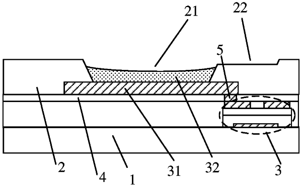
1. An organic light-emitting diode display substrate having a plurality of pixel regions, comprising a base substrate, and a pixel defining layer disposed on the base substrate; wherein, in regions of the pixel defining layer, which correspond to the pixel regions, there are disposed accommodation parts which penetrate the pixel defining layer in a direction perpendicular to the base substrate, the pixel defining layer is further provided with guide parts disposed corresponding to the accommodation parts,
the guide parts are located on a periphery of the corresponding accommodation parts and are formed by recessed areas which are formed at positions on a side of the pixel defining layer away from the base substrate, the recessed areas do not penetrate the pixel defining layer in the direction perpendicular to the base substrate, and
an orthographic projection of the guide part on the base substrate is directly coupled to an orthographic projection of the corresponding accommodation part on the base substrate.
|