| CPC H10B 63/30 (2023.02) [H01L 21/02532 (2013.01); H01L 21/02603 (2013.01); H01L 29/0673 (2013.01); H01L 29/42392 (2013.01); H01L 29/66439 (2013.01); H01L 29/66545 (2013.01); H01L 29/66742 (2013.01); H01L 29/775 (2013.01); H01L 29/78696 (2013.01); H10N 70/011 (2023.02); H10N 70/24 (2023.02)] | 7 Claims |

|
1. A microelectronic system comprising a plurality of microelectronic devices, wherein
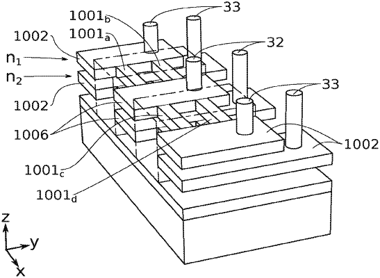
each of the devices comprises at least two transistors each comprising a channel in the shape of a wire extending mainly in a first direction x, a gate surrounding said channel, a source and a drain associated with the channel, said transistors being stacked in a third direction z so that the channels of said transistors each occupy a level nz (z=1 . . . 4) of given altitude in the third direction z, wherein, for each channel of level nz of given altitude, the source and the drain associated with said channel are located only at said level nz, and the gate is bordered by longitudinal spacers, said longitudinal spacers extending on either side of the gate mainly in a second direction v normal to the first and third directions x, z, said longitudinal spacers covering an upper surface of the source and the drain of each transistor;
said devices are adjacent along a normal plane comprising the third direction z; and
the sources and/or the drains of a level nz of given altitude of two adjacent devices are shared between said two adjacent devices.
|