| CPC H10B 43/50 (2023.02) [H01L 21/76805 (2013.01); H01L 21/76895 (2013.01); H01L 23/535 (2013.01); H10B 41/27 (2023.02); H10B 41/41 (2023.02); H10B 41/50 (2023.02); H10B 43/27 (2023.02); H10B 43/40 (2023.02)] | 18 Claims |
|
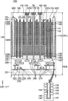
1. A semiconductor device, comprising:
a peripheral circuit region including a first substrate and circuit devices on the first substrate;
a memory cell region including a second substrate on the first substrate, gate electrodes stacked in a first direction perpendicular to an upper surface of the second substrate and spaced apart from each other, and channel structures extending in the gate electrodes in the first direction, each of the channel structures including a channel layer; and
a through wiring region adjacent to the channel structures and electrically connecting the peripheral circuit region to the memory cell region,
wherein the through wiring region includes:
an insulating region side by side with the second substrate and the gate electrodes;
a through contact plug extending through the insulating region in the first direction; and
dummy channel structures partially extending into an upper portion of the insulating region, each of the dummy channel structures including the channel layer,
wherein each of the channel structures has a first height in the first direction, and each of the dummy channel structures has a second height smaller than the first height, and
wherein the channel structures are arranged with a first pitch in a second direction perpendicular to the first direction, and the dummy channel structures are arranged with a second pitch different from the first pitch in the second direction in a region adjacent to at least one of the channel structures.
|