| CPC H10B 43/40 (2023.02) [G11C 5/025 (2013.01); G11C 7/06 (2013.01); G11C 16/08 (2013.01); G11C 16/16 (2013.01); G11C 16/24 (2013.01); G11C 16/26 (2013.01); H01L 24/05 (2013.01); H01L 24/20 (2013.01); H10B 43/10 (2023.02); H10B 43/35 (2023.02); H01L 2924/1438 (2013.01)] | 13 Claims |
|
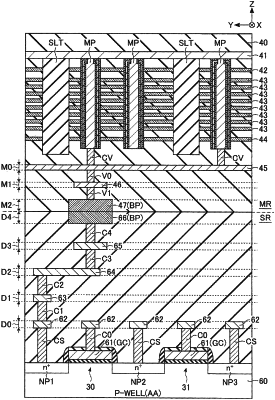
1. A semiconductor memory device comprising:
a substrate including a first region and a second region;
a plurality of first transistors provided in the first region;
a plurality of second transistors provided in the second region, the plurality of second transistors being electrically coupled to the plurality of first transistors, respectively, and a breakdown-voltage of the second transistors being lower than a breakdown-voltage of the first transistors;
a plurality of joint metals provided above the first region, the plurality of joint metals being electrically coupled to the plurality of first transistors, respectively;
a plurality of bit lines provided in an upper layer with respect to the plurality of joint metals, the plurality of bit lines being coupled to the plurality of joint metals, respectively; and
a plurality of memory cells provided in an upper layer with respect to the plurality of bit lines, the plurality of memory cells being coupled to the plurality of bit lines, respectively,
wherein the first transistors and the plurality of joint metals overlap in a planar view, and a pitch of the plurality of joint metals in a first direction approximately doubles a pitch of a first transistor in the first direction.
|