| CPC H10B 43/27 (2023.02) [H10B 41/27 (2023.02); H10B 41/40 (2023.02); H10B 43/40 (2023.02)] | 28 Claims |
|
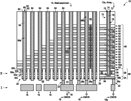
1. An integrated assembly, comprising:
a memory array region and another region proximate the memory array region;
conductive structures distributed along a level within the memory array region and the another region; the conductive structures including a metal-containing region and a first stack over the metal-containing region; the first stack including alternating semiconductor-material-containing regions and intervening regions; one of the semiconductor-material-containing regions being a central semiconductor-material-containing region and being vertically between two others of the semiconductor-material-containing regions;
a second stack over the level and over the conductive structures; the second stack comprising alternating first and second tiers; the first tiers comprising conductive material and the second tiers comprising insulative material;
cell-material-pillars within the memory array region; the cell-material-pillars extending through the second stack and into the first stack; the cell-material-pillars including channel material and including other materials laterally outward of the channel material; the central semiconductor material penetrating laterally through the other materials and directly contacting the channel material; and
conductive post structures within the another region; the conductive post structures extending through the second stack and through the conductive structures; some of the conductive post structures being dummy structures and having bottom surfaces which are entirely along an insulative oxide material, and others of the conductive post structures being live structures and being electrically coupled with CMOS circuitry which is beneath the level.
|