| CPC H10B 41/27 (2023.02) [G11C 5/025 (2013.01); G11C 5/06 (2013.01); H01L 25/074 (2013.01); H01L 29/66666 (2013.01); H10B 43/27 (2023.02)] | 20 Claims |
|
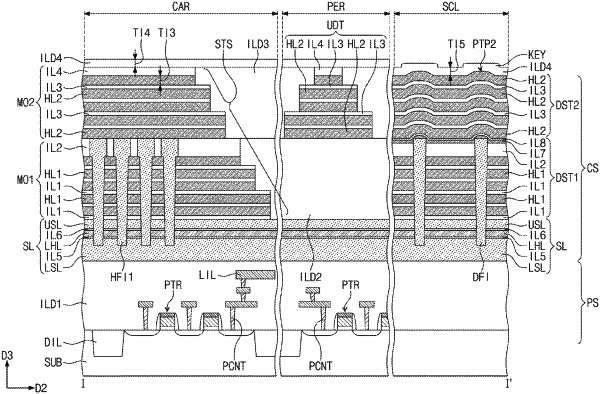
1. A semiconductor device, comprising:
a substrate including a cell array region and a key region;
a stack structure on the cell array region, wherein the stack structure includes a first stack structure on the substrate and a second stack structure on the first stack structure, each of the first and second stack structures including a vertically stacked and spaced apart electrodes;
a dummy structure on the key region, wherein the dummy structure includes a first dummy structure on the substrate and a second dummy structure on the first dummy structure;
a vertical channel structure penetrating the stack structure to connect the substrate;
a dummy pillar penetrating the first dummy structure, wherein an upper portion of the dummy pillar protrudes upwardly from an upper surface of the first dummy structure, and the second dummy structure conforms to the first dummy structure such that an upper surface of the second dummy structure includes an upwardly extending protrusion aligned over the dummy pillar;
an interlayer dielectric layer on the stack structure and the dummy structure, wherein an upper portion of the interlayer dielectric layer on the dummy structure includes a key pattern that vertically overlaps the upwardly extending protrusion of the second dummy structure; and
a capping layer on the key region and covering the key pattern.
|
|
12. An electronic system, comprising:
a semiconductor device including an input/output pad electrically connected to a peripheral circuit; and
a controller electrically connected through the input/output pad to the semiconductor device and configured to control the semiconductor device,
wherein the semiconductor device includes:
a substrate including a cell array region and a key region;
a stack structure on the cell array region, the stack structure including vertically stacked and spaced apart electrodes;
a dummy structure on the key region, wherein an upper surface of the dummy structure includes a plurality of upwardly extending protrusions;
a vertical channel structure penetrating the stack structure to connect the substrate;
an interlayer dielectric layer on the stack structure and the dummy structure, wherein the interlayer dielectric layer on the upper surface of the dummy structure conforms with the upper surface of the dummy structure and includes a key pattern vertically overlapping the plurality of upwardly extending protrusions of the dummy structure, and a top surface of the interlayer dielectric layer on the stack structure is higher than a top surface of the interlayer dielectric layer on the dummy structure; and
a capping layer on the key region and covering the key pattern, wherein the capping layer includes polysilicon.
|
|
18. A semiconductor device, comprising:
a substrate including a cell array region and a key region;
a stack structure on the cell array region, wherein the stack structure includes a first stack structure on the substrate and a second stack structure on the first stack structure, each of the first and second stack structures including a vertically stacked and spaced apart electrodes;
a dummy structure on the key region, wherein the dummy structure includes a first dummy structure on the substrate and a second dummy structure on the first dummy structure;
a vertical channel structure penetrating the stack structure to connect the substrate;
a dummy pillar penetrating the first dummy structure;
an interlayer dielectric layer on the stack structure and the dummy structure, wherein an upper portion of the interlayer dielectric layer on the dummy structure includes a key pattern that vertically overlaps the dummy pillar;
a capping layer on the key region and covering the key pattern; and
an upper dummy structure on a peripheral region of the substrate, wherein the peripheral region is disposed between the cell array region and the key region, and the upper dummy structure is at a same level as the second stack structure and the second dummy structure.
|