| CPC H10B 41/27 (2023.02) [H10B 41/35 (2023.02); H10B 41/41 (2023.02); H10B 43/27 (2023.02); H10B 43/35 (2023.02); H10B 43/40 (2023.02)] | 21 Claims |
|
1. An integrated circuit structure, comprising:
a semiconductor material;
a first active area in the semiconductor material;
a second active area in the semiconductor material; and
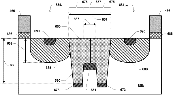
an isolation structure comprising a dielectric material deposited in a trench formed in the semiconductor material between the first active area and the second active area, the isolation structure further comprising:
a first edge portion extending below a surface of the semiconductor material to a first depth;
a second edge portion extending below the surface of the semiconductor material to the first depth; and
an interior portion between the first edge portion and the second edge portion, and extending below the surface of the semiconductor material to a second depth, less than the first depth, for a distance that is greater than or equal to an attribute of the first active area selected from a group consisting of a width of the first active area and a length of the first area.
|