| CPC H10B 41/27 (2023.02) [G11C 7/18 (2013.01); G11C 8/14 (2013.01); H01L 29/0653 (2013.01); H10B 41/10 (2023.02); H10B 41/35 (2023.02); H10B 43/10 (2023.02); H10B 43/27 (2023.02); H10B 43/35 (2023.02)] | 18 Claims |
|
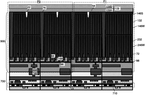
1. A three-dimensional memory device, comprising:
an alternating stack of insulating layers and electrically conductive layers located over a plurality of source layers, wherein the alternating stack is located between a pair of backside trench fill structures, wherein the electrically conductive layers comprise word lines and source-side select gate electrodes which are located between the plurality of source layers and the word lines in a vertical direction,
source-side trenches extending through both the source-side select gate electrodes and the plurality of source layers, wherein the source-side trenches do not divide the word lines;
groups of memory openings vertically extending through the alternating stack; and
groups of memory opening fill structures located in the groups of memory openings, wherein each of the memory opening fill structures includes a respective vertical stack of memory elements, a respective vertical semiconductor channel having a first end that contacts a respective one of the plurality of source layers, and a respective drain region contacting a second end of the respective vertical semiconductor channel,
wherein:
the plurality of source layers are laterally spaced apart and electrically isolated from each other; and
each group of memory opening fill structures contacts a respective one of the plurality of source layers.
|