| CPC H10B 12/038 (2023.02) [H01L 28/60 (2013.01)] | 12 Claims |

|
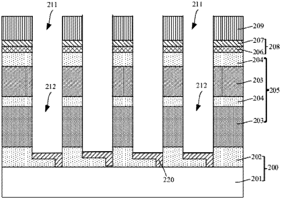
1. A method for forming capacitor holes, comprising:
providing a semiconductor base in which a plurality of connecting pads are formed;
forming a supporting layer on the semiconductor base;
forming an over-etching depth adjusting layer on the supporting layer, wherein the over-etching depth adjusting layer comprises a first material layer on the supporting layer and a second material layer on the first material layer, the first material layer and the second material layer are different in materials and different from a hard mask layer formed subsequently in materials, and the first material layer and the second material layer are both thinner than the hard mask layer formed subsequently;
forming the hard mask layer on the over-etching depth adjusting layer;
etching the hard mask layer to form a plurality of etching holes, and when etching the hard mask layer to form the etching holes, over-etching the hard mask layer to reach a certain over-etching depth in the second material layer, and making the etching holes terminate in the first material layer; and
etching the first material layer and the supporting layer along the etching holes to form a plurality of capacitor holes exposing surfaces of the respective connecting pads in the supporting layer.
|