| CPC H10B 12/033 (2023.02) [H10B 12/31 (2023.02)] | 14 Claims |

|
1. A method for manufacturing a capacitor, comprising:
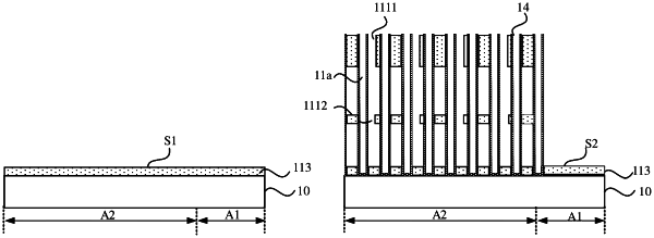
providing a wafer, the wafer comprising a plurality of dies distributed in an array, and the dies having a same underlayer; forming a substrate to be etched on the underlayer, the substrate to be etched comprising at least one sacrificial layer and at least one support layer, the sacrificial layer and the support layer being alternately arranged, and one side, away from the underlayer, of the substrate to be etched being a first support layer;
enabling the wafer to comprise a central area and an edge area surrounding the central area;
removing a portion, for dies in the edge area, of the first support layer;
forming a first hard mask layer having a first pattern in the central area on the substrate to be etched, the first pattern comprising through holes arranged in an array, and no through hole being formed in a part of the first hard mask layer corresponding to the edge area; using the first hard mask layer as a mask to etch the substrate to be etched, to form capacitor holes in the central area, no capacitor hole being formed in an array region and a peripheral region of each of the dies in the edge area; and
depositing a lower electrode layer on a bottom and a side wall of each of the capacitor holes, and removing, layer by layer, part of the substrate to be etched; and sequentially forming a capacitor dielectric layer and an upper electrode layer on the lower electrode layer.
|