| CPC H10B 10/12 (2023.02) [H01L 21/02532 (2013.01); H01L 21/0332 (2013.01); H01L 21/324 (2013.01); H01L 21/823807 (2013.01); H01L 21/823814 (2013.01); H01L 21/823821 (2013.01); H01L 21/823828 (2013.01); H01L 27/0924 (2013.01); H01L 29/161 (2013.01); H01L 29/165 (2013.01); H01L 29/495 (2013.01); H01L 29/4966 (2013.01); H01L 29/66545 (2013.01); H01L 21/02236 (2013.01); H01L 21/02255 (2013.01); H01L 29/517 (2013.01)] | 20 Claims |

|
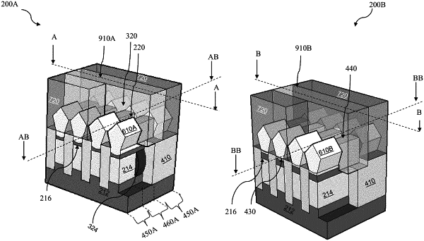
1. A method, comprising:
providing a substrate comprising a first semiconductor layer, a second semiconductor layer over the first semiconductor layer, and a third semiconductor layer disposed over the second semiconductor layer;
forming a fin structure over the substrate, wherein the fin structure comprising a lower portion formed of the first semiconductor layer, a middle portion formed of the second semiconductor layer, and a top portion formed of the third semiconductor layer;
forming a patterned mask layer to cover a source/drain region of the fin structure while a channel region of the fin structure is exposed;
after the forming of the patterned mask layer, oxidizing the channel region of the fin structure to form a first oxide feature over sidewalls of the lower portion, a second oxide feature over sidewalls of the middle portion, and a third oxide feature over sidewalls of the top portion;
removing the first oxide feature and the third oxide feature;
depositing a first dielectric layer over the fin structure;
recessing the first dielectric layer to expose at least a portion of the top portion;
forming a dummy gate structure over the channel region;
forming a source/drain feature over the source/drain region;
depositing a second dielectric layer over the source/drain feature; and
replacing the dummy gate structure with a metal gate structure.
|