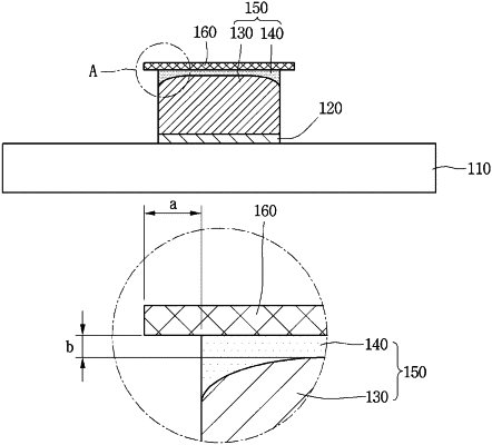
|
1. A circuit board comprising: an insulating layer including an upper surface and a lower surface opposite to the upper surface; a circuit layer disposed on the upper surface of the insulating layer; and a top metal layer disposed on the circuit layer, wherein the circuit layer includes a portion that is positioned higher than an upper surface of the insulating layer with respect to the lower surface of the insulating layer, wherein the top metal layer is disposed on the portion of the circuit layer, wherein the top metal layer includes a first portion, and a second portion extended outwards from the first portion, wherein the first portion is vertically overlapped with the portion of the circuit layer and is in direct physical contact with the portion of the circuit layer, wherein the second portion is not in contact with the portion of the circuit layer and does not vertically overlap with the portion of the circuit layer, wherein the top metal layer is formed of gold or a gold alloy; wherein the portion of the circuit layer includes a first layer and a second layer disposed on the first layer, wherein a thickness of the first layer is greater than a thickness of the second layer, and wherein the first layer and the second layer include a same metal material.
|
