| CPC H05K 1/0231 (2013.01) [H05K 1/0225 (2013.01); H05K 1/0233 (2013.01); H05K 2201/1006 (2013.01); H05K 2201/10015 (2013.01)] | 9 Claims |

|
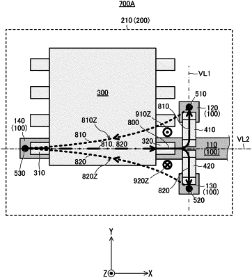
1. A circuit board comprising a stack of a first conductive layer and a second conductive layer each having electrical conductivity provided with an insulating layer having an electrical insulating property therebetween, the circuit board being provided with a semiconductor device thereon, the semiconductor device comprising a reference terminal to provide a reference potential and a non-reference terminal to output a signal, the circuit board comprising:
a wiring member included in the first conductive layer;
a first capacitor and a second capacitor, each of the capacitors comprising one terminal connected to the wiring member;
a reference member included in the second conductive layer;
a first interlayer joint to electrically connect the reference member to another terminal of the first capacitor;
a second interlayer joint to electrically connect the reference member to another terminal of the second capacitor; and
a third interlayer joint to electrically connect the reference member to the reference terminal, with the semiconductor device mounted on the circuit board, wherein
the first capacitor extends from the wiring member to a region located on one side of the wiring member in a width direction thereof, and the second capacitor extends from the wiring member to a region located on another side of the wiring member in the width direction, and
with the semiconductor device mounted on the circuit board,
the non-reference terminal is electrically connected to the wiring member,
the semiconductor device, the wiring member, the first capacitor, the first interlayer joint, the reference member, and the third interlayer joint constitute a first closed circuit, and
the semiconductor device, the wiring member, the second capacitor, the second interlayer joint, the reference member, and the third interlayer joint constitute a second closed circuit.
|