| CPC H04N 25/772 (2023.01) [H01L 27/14 (2013.01); H01L 27/146 (2013.01); H01L 27/14603 (2013.01); H01L 27/14609 (2013.01); H01L 27/14634 (2013.01); H01L 27/14636 (2013.01); H01L 27/14643 (2013.01); H01L 27/14645 (2013.01); H04N 23/65 (2023.01); H04N 25/70 (2023.01); H04N 25/745 (2023.01); H04N 25/75 (2023.01); H04N 25/76 (2023.01); H04N 25/79 (2023.01); G01S 17/10 (2013.01); H01L 27/1464 (2013.01); H01L 27/14621 (2013.01); H01L 27/14627 (2013.01); H04N 25/709 (2023.01)] | 14 Claims |
|
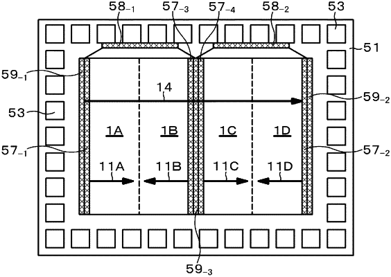
1. An imaging device comprising:
a first substrate including a pixel array unit which has a first pixel array, a second pixel array, and a third pixel array;
a second substrate bonded to the first substrate, the second substrate including a first pixel row control circuit, a second pixel row control circuit, a third pixel row control circuit, and a column processing unit wherein:
the first pixel array is electrically connected to the first pixel row control circuit, the second pixel array is electrically connected to the second pixel row control circuit, and the third pixel array is electrically connected to the third pixel row control circuit;
wherein: each of the first pixel array, the second pixel array and the third pixel array comprises a plurality of pixels arranged in a plurality of columns and a plurality of rows;
wherein: each of the first pixel row control circuit, the second pixel row control circuit and the third pixel row control circuit is configured to control a respective plurality of rows of pixels of the first pixel array, the second pixel array and the third pixel array;
wherein: the first pixel row control circuit, the second pixel row control circuit, and the third pixel row control circuit are physically separated from one another on the second substrate; and
wherein: the column processing unit is distributed among the first pixel row control circuit and the second pixel row control circuit.
|