| CPC H04N 25/75 (2023.01) [H01L 27/14612 (2013.01); H01L 27/14643 (2013.01); H04N 25/59 (2023.01); H04N 25/778 (2023.01)] | 19 Claims |

|
1. A method for pixel-embedded signal amplification of a CMOS image sensor using multi-step voltage gain enhancement, the method comprising:
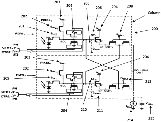
activating ROW1 of the CMOS image sensor by resetting a plurality of switches SRST, SH1 and SH2 to charge nodes PD1, PD2, SD1, and SD2 to a pre-set voltage potential and VRST respectively;
switching the plurality of switches OFF SRST, SH1 and SH2 for integration of photo-generated charges at node PD1 for producing a corresponding photo generated signal;
sampling the photo generated signal by transferring the said signal to a gate of source follower SF1, to produce an amplified photo generated signal;
double sampling the amplified photo generated signal in column for removing any pixel offset variation to produce a resultant voltage signal;
activating ROW2 of the CMOS image sensor by resetting the plurality of switches SRST, SH1 and SH2 to charge nodes PD1, PD2, SD1, and SD2 to the pre-set voltage potential and VRST respectively;
switching the plurality of switches OFF SRST, SH1 and SH2 for integration of photo-generated charges at node PD2 for producing a corresponding photo generated signal;
sampling the photo generated signal by transferring the said signal to a gate of source follower SF2, to produce an amplified photo generated signal;
double sampling the amplified photo generated signal in column for removing any pixel offset variation for implementing multiple steps of gain on the resultant voltage signal; and
converting the resultant voltage to digital bits to obtain an output signal of with enhanced gain.
|