| CPC H04N 25/75 (2023.01) [H01L 27/14612 (2013.01); H01L 27/14636 (2013.01); H01L 27/14643 (2013.01); H04N 25/766 (2023.01)] | 21 Claims |
|
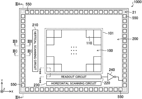
1. A light detector in which a light receiving portion having one or more avalanche photodiodes and a peripheral circuit portion exchanging a signal with the light receiving portion are provided on a first principal surface of a first conductive type semiconductor substrate, comprising at least:
a back electrode provided on a second principal surface of the semiconductor substrate facing the first principal surface and configured to apply a predetermined voltage to the semiconductor substrate; and
a first conductive type first separation portion provided between the light receiving portion and the peripheral circuit portion with a predetermined interval from each of the light receiving portion and the peripheral circuit portion in a direction parallel with the first principal surface,
wherein each avalanche photodiode has at least
a second conductive type first region provided to extend inward of the semiconductor substrate from the first principal surface, and
a first conductive type second region provided in contact with the first region in a direction crossing the first principal surface, and
the peripheral circuit portion has at least
a first conductive type first well provided to extend inward of the semiconductor substrate from the first principal surface,
a first transistor provided at the first well, and
a second conductive type third well provided to surround side and bottom portions of the first well.
|