| CPC H04N 25/709 (2023.01) [H04N 25/772 (2023.01)] | 20 Claims |

|
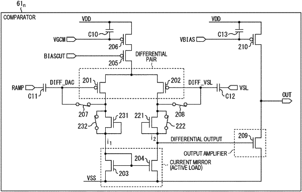
1. An imaging device comprising:
a differential pair comprising:
a first transistor configured to receive a pixel signal from a pixel circuit, and
a second transistor configured to receive a reference signal from a reference signal output circuit;
a current mirror electrically connected to a first power source;
a first voltage drop transistor electrically connected between the current mirror and the first transistor;
a second voltage drop transistor electrically connected between the current mirror and the second transistor;
a first switch electrically connected in parallel to the first voltage drop transistor;
a second switch electrically connected in parallel to the second voltage drop transistor; and
a current source electrically connected to the differential pair, wherein
the current source comprises a third transistor, a fourth transistor and a capacitor,
the third transistor is electrically connected to the first transistor and the second transistor,
the fourth transistor is electrically connected to the third transistor and a second power source which is lower voltage than the first power source, and
the capacitor is electrically connected to a gate of the fourth transistor and the second power source.
|