| CPC H04N 25/68 (2023.01) [H04N 25/772 (2023.01)] | 24 Claims |

|
1. An electronic device, comprising:
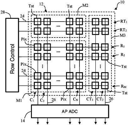
a first array of image pixels having inputs coupled to first selection tracks and outputs coupled to first output tracks;
at least one second array of test pixels having inputs coupled to second selection tracks and outputs coupled to the first output tracks;
at least one third array of test pixels having inputs coupled to the first selection tracks and outputs coupled to second output tracks; and
a processor coupled to receive output signals on the first and second output tracks;
wherein each test pixel of the second and third arrays is configured to generate the output signal at one of only two possible reference voltage values set by a circuit connection of the test pixel in the absence of a selection track defect or output track defect; and
wherein the processor is configured to identify existence of the selection track defect or output track defect in response to the output signal received from one or a plurality of the test pixels having a value other than said one of the two possible reference voltage values set by the circuit connection.
|