| CPC H04N 23/745 (2023.01) [G06T 5/001 (2013.01); G06T 5/50 (2013.01); G06T 7/20 (2013.01); G06V 10/60 (2022.01); G06T 2207/20212 (2013.01); H01L 27/1464 (2013.01); H01L 27/14621 (2013.01); H01L 27/14623 (2013.01); H01L 27/14627 (2013.01); H01L 27/14636 (2013.01); H01L 27/14645 (2013.01)] | 18 Claims |
|
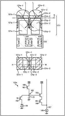
1. An imaging device comprising:
a pixel region in which a plurality of pixels including a pixel that receives incident light and outputs one detection signal indicating an output pixel value modulated depending on an incident angle of the incident light is arranged in a row direction and a column direction, and is sequentially exposed row by row, the incident light entering from an object via neither an imaging lens nor a pinhole; and
a plurality of detection regions that are disposed in different rows in the pixel region, and are used for flicker detection.
|