| CPC H04B 7/0456 (2013.01) [H04B 1/0483 (2013.01); G06K 19/0723 (2013.01); H04B 2001/0408 (2013.01)] | 14 Claims |
|
1. A system for signal processing, comprising:
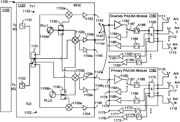
a radio frequency integrated circuit (RFIC) having a plurality of available transmission paths, the RFIC configured to have at least a first communication signal on a first transmission path of the available transmission paths;
a plurality of power amplifier and low noise amplifier (PA/LNA) modules selectively connected to the RFIC, each of the PA/LNA modules configured to connect to at least one respective antenna; and
switch logic configured to connect the at least first communication signal to any of the plurality of PA/LNA modules prior to power amplification, while preventing the first communication signal from affecting or being affected by another communication signal on another of the plurality of available transmission paths,
wherein the switch logic comprises baseband switch logic, wherein a local oscillator (LO) input and a baseband input are switched between the first transmission path and the another of the plurality of available transmission paths respectively prior to mixing.
|