| CPC H04B 10/672 (2013.01) [H04B 10/29 (2013.01); H04B 10/40 (2013.01); H04B 10/50 (2013.01); H04B 10/60 (2013.01)] | 7 Claims |
|
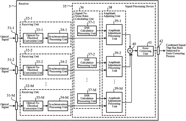
1. A signal processing device to process reception signals of optical signals received by a receiver when the optical signals transmitted from a transmitter are propagated to the receiver via a plurality of paths, the signal processing device comprising:
signal-to-noise ratio calculating circuitry to calculate signal-to-noise ratios of the optical signals that have been propagated through the respective paths, the signal-to-noise ratios being based on propagation distances of the optical signals in the respective paths, intensities of the optical signals transmitted from the transmitter, and intensities of noise with respect, to the optical signals transmitted from the transmitter;
amplitude adjusting circuitry to adjust amplitudes of the reception signals of the optical signals that have been propagated through the respective paths, using the corresponding signal-to-noise ratios calculated by the signal-to-noise ratio calculating circuitry; and
signal combining circuitry to combine the reception signals whose amplitudes have been adjusted by the amplitude adjusting circuitry.
|