US 11,888,530 B2
Optical tracking module chip for wireless optical communication terminal
Baris Ibrahim Erkmen, Sunnyvale, CA (US); Devin Brinkley, Redwood City, CA (US); Eric Teller, Palo Alto, CA (US); Thomas Moore, Menlo Park, CA (US); and Jean-Laurent Plateau, San Jose, CA (US)
Assigned to X DEVELOPMENT LLC, Mountain View, CA (US)
Filed by X DEVELOPMENT LLC, Mountain View, CA (US)
Filed on Mar. 18, 2022, as Appl. No. 17/698,224.
Claims priority of provisional application 63/246,599, filed on Sep. 21, 2021.
Claims priority of provisional application 63/246,605, filed on Sep. 21, 2021.
Prior Publication US 2023/0088334 A1, Mar. 23, 2023
Int. Cl. H04B 10/61 (2013.01); G01S 7/481 (2006.01); G02F 1/29 (2006.01); G02B 27/00 (2006.01); G01S 17/66 (2006.01)
CPC H04B 10/614 (2013.01) [G01S 7/4817 (2013.01); G01S 17/66 (2013.01); G02B 27/0087 (2013.01); G02F 1/292 (2013.01)] 20 Claims
OG exemplary drawing
 
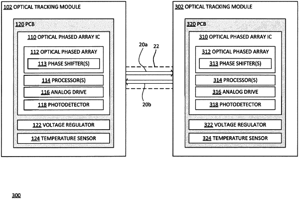
1. An optical tracking module comprising:
an optical phased array (OPA) including:
a plurality of array elements, and
a plurality of phase shifters;
an analog drive configured to adjust the plurality of phase shifters;
an integrated photodetector configured to receive light from the OPA; and
one or more processors configured to:
extract signal information of an incoming beam via the OPA, and
control an outgoing beam using the analog drive based on the signal information; and
wherein the OPA, the analog drive, the integrated photodetector and the one or more processors are in an integrated circuit.