| CPC H03L 7/0818 (2013.01) [G11C 7/222 (2013.01); G11C 7/225 (2013.01); H03L 7/083 (2013.01); H03L 7/0814 (2013.01); H03L 7/0816 (2013.01)] | 20 Claims |

|
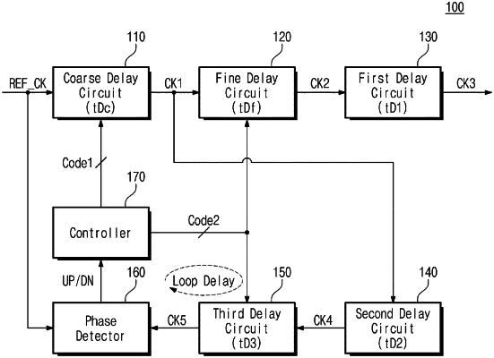
1. A delay locked loop apparatus, comprising:
a coarse delay circuit configured to delay a reference clock signal to generate a first clock signal;
a fine delay circuit configured to delay the first clock signal to generate a second clock signal;
a first delay circuit configured to delay the second clock signal to generate a third clock signal;
a second delay circuit configured to delay the first clock signal to generate a fourth clock signal;
a third delay circuit configured to delay the fourth clock signal to generate a fifth clock signal;
a phase detector configured to detect a phase difference between the reference clock signal and the fifth clock signal; and
a controller configured to adjust, based on a detection result of the phase detector, a first delay amount of the coarse delay circuit, a second delay amount of the fine delay circuit and a third delay amount of third delay circuit.
|