| CPC H03K 5/01 (2013.01) [H03H 11/16 (2013.01); H03K 2005/00019 (2013.01)] | 18 Claims |

|
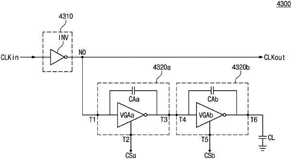
1. A phase correcting circuit, comprising:
a delay circuit configured to receive an input clock signal and to delay the input clock signal as much as a first delay time to output an output clock signal to a 0-th node;
a first fine tuning circuit including a first terminal connected with the 0-th node, a second terminal receiving a first control signal, and a third terminal; and
a second fine tuning circuit including a fourth terminal connected with the third terminal, a fifth terminal receiving a second control signal, and a sixth terminal connected with a load capacitor;
wherein, in response to the first control signal, the output clock signal is further delayed as much as a second delay time shorter than the first delay time; and
wherein, in response to the second control signal, the output clock signal is advanced as much as a third delay time shorter than the first delay time; and
wherein a magnitude of the third delay time is smaller than a magnitude of the second delay time.
|