| CPC H03K 3/017 (2013.01) [H03F 3/45475 (2013.01); H03H 11/04 (2013.01)] | 18 Claims |

|
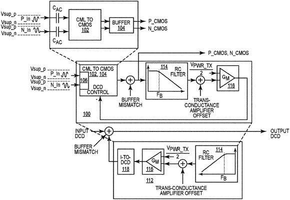
1. A clock signal conversion circuit, comprising:
an amplification circuit configured to amplify a differential clock signal that has sub rail-to-rail voltage swings relative to a supply voltage for the amplification circuit, such that an amplified differential clock signal output by the amplification circuit has complementary positive and negative signal components with full rail-to-rail voltage swings relative to the supply voltage; and
a duty cycle distortion correction circuit comprising:
a filter having a cutoff frequency below the frequency of the differential clock signal and configured to output a differential voltage that is proportional to a difference in duty cycle between the positive and negative signal components of the amplified differential clock signal;
a transconductance amplifier configured to convert the differential voltage to a differential current that is provided to the amplification circuit as feedback for reducing the duty cycle difference between the positive and negative signal components of the amplified differential clock signal; and
a common-mode loop comprising a PMOS transistor having a gate driven by a mid-rail voltage reference, wherein the common-mode loop is configured to force the average of a positive side of the differential voltage and a negative side of the differential voltage to half the mid-rail voltage reference.
|