| CPC H03K 19/0005 (2013.01) [G11C 7/1048 (2013.01); G11C 7/1051 (2013.01)] | 12 Claims |

|
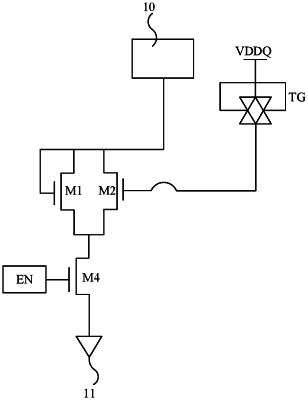
1. An on die termination (ODT) circuit, comprising:
a signal input terminal;
a grounding terminal;
a first transistor, comprising a control terminal, a first terminal and a second terminal, wherein the control terminal of the first transistor and the first terminal of the first transistor are electrically connected with the signal input terminal, and the second terminal of the first transistor is electrically connected with the grounding terminal; and
a second transistor, comprising a control terminal, a first terminal and a second terminal, wherein the first terminal of the second transistor is electrically connected with the signal input terminal, the second terminal of the second transistor is electrically connected with the grounding terminal, and in response to a change in a voltage of the signal input terminal, a change trend of a resistance of the first transistor is opposite to a change trend of a resistance of the second transistor;
wherein:
the first transistor works in a saturation region, and the change trend of the resistance of the first transistor is at least one of following: the resistance of the first transistor decreases as the voltage of the signal input terminal increases, or the resistance of the first transistor increases as the voltage of the signal input terminal decreases; and
the second transistor works in a linear region, and the change trend of the resistance of the second transistor is at least one of following: the resistance of the second transistor increases as the voltage of the signal input terminal increases, or the resistance of the second transistor decreases as the voltage of the signal input terminal decreases.
|