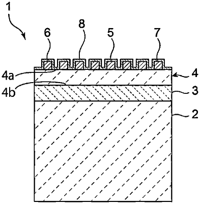
1. An acoustic wave device comprising:
a silicon support substrate;
a silicon oxide film laminated above the silicon support substrate;
a lithium tantalate film laminated above the silicon oxide film;
an IDT electrode including an electrode finger and being provided above the lithium tantalate film; and
a protection film covering at least a portion of the IDT electrode; wherein
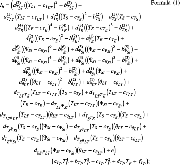
when a wavelength determined by an electrode finger pitch of the IDT electrode is denoted by λ, a wavelength normalized film thickness of the lithium tantalate film is denoted by TLT, θ of an Euler angle of the lithium tantalate film is denoted by θLT, a wavelength normalized film thickness of the silicon oxide film is denoted by TS, a wavelength normalized film thickness of the IDT electrode in terms of aluminum thickness being a product of a wavelength normalized film thickness of the IDT electrode and a value obtained when density of the IDT electrode is divided by density of aluminum is denoted by TE, a wavelength normalized film thickness of the protection film being a product of a value obtained when density of the protection film is divided by density of silicon oxide and a wavelength normalized film thickness which is a thickness of the protection film normalized by the wavelength λ is denoted by TP, a propagation direction in the silicon support substrate is denoted by ψSi, and a wavelength normalized film thickness which is a thickness of the silicon support substrate normalized by the wavelength λ is denoted by TSi, TLT, θLT, TS, TE, TP, and ψSi are set such that a value represented by Formula (1) below is larger than about −2.4:
where, coefficients a, b, c, d, e, and f in Formula (1) are values described in Table 1 to Table 12 below that are determined in accordance with a crystal orientation of the silicon support substrate and a range of TS, TLT, and ψSi: