| CPC H03F 1/523 (2013.01) [H03F 1/0222 (2013.01); H03F 1/223 (2013.01); H03F 3/195 (2013.01); H03F 3/245 (2013.01); H03F 3/72 (2013.01); H03F 2200/294 (2013.01); H03F 2200/435 (2013.01); H03F 2200/451 (2013.01)] | 18 Claims |

|
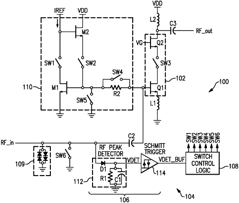
1. An amplifier circuit comprising:
an input node and an output node;
an amplifier implemented between the input node and the output node, the amplifier including a cascade arrangement of a first transistor and a second transistor, the first transistor having an input coupled to the input node, the second transistor coupled to the first transistor and having an output coupled to the output node;
a bias circuit configured to provide a bias signal to the amplifier; and
a protection circuit configured to generate a detected voltage representative of a peak of a radio-frequency signal present at the input node, the protection circuit further configured to enable a protection mode when the detected voltage is greater than a first threshold value and to disable the protection mode when the detected voltage is less than a second threshold value that is less than the first threshold value, the protection circuit including an assembly of one or more switches configured to implement the enablement and disablement of the protection mode.
|