| CPC H02M 7/4835 (2021.05) [H02M 1/08 (2013.01); H02M 1/32 (2013.01); H02M 3/33523 (2013.01); H02M 7/483 (2013.01); H02M 7/4833 (2021.05)] | 20 Claims |
|
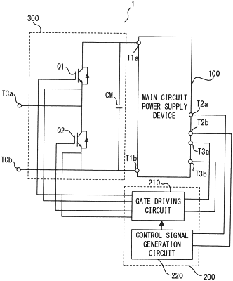
1. A power conversion device comprising:
a main circuit including a main circuit switching element and a main circuit power storage element;
main circuit control circuitry to control the main circuit; and
a main circuit power supply device to supply a control power source from the main circuit power storage element to the main circuit control circuitry, wherein
the main circuit power supply device includes
a plurality of voltage-division power storage elements connected in series,
a voltage adjustment circuit which is connected to the plurality of voltage-division power storage elements and adjusts each of voltages of the plurality of voltage-division power storage elements through mutual transfer of power between the plurality of voltage-division power storage elements, and
at least one DC/DC converter which is connected to at least one of the plurality of voltage-division power storage elements and supplies the control power source.
|