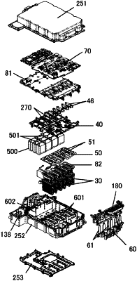
| CPC H02M 7/003 (2013.01) [H01L 23/34 (2013.01); H02M 7/537 (2013.01); H05K 7/1432 (2013.01); H05K 7/209 (2013.01)] | 7 Claims |

|
1. A power conversion device comprising:
a capacitor;
a first power semiconductor module and a second power semiconductor module each having an input terminal or an output terminal protruding from one surface;
a case including a capacitor housing portion that houses the capacitor, a semiconductor module housing portion that houses the first power semiconductor module and the second power semiconductor module, and a partition portion provided between the first power semiconductor module and the second power semiconductor module; and
a connection member in which a resin portion and a connection conductor are integrally provided and which is disposed on the one surface of the first power semiconductor module and the second power semiconductor module, wherein
the connection conductor includes a capacitor connection portion connected to the capacitor, a first terminal portion exposed from the resin portion and connected to the terminal of the first power semiconductor module, and a second terminal portion connected to the terminal of the second power semiconductor module,
the partition portion of the case is provided with a protruding portion that protrudes toward the connection member further than the one surface of the first power semiconductor module and the second power semiconductor module and is thermally coupled to the connection member, and
the protruding portion is thermally coupled to the connection member and disposed between a first root portion of an exposed portion where the first terminal portion is exposed from the resin portion and a second root portion of an exposed portion where the second terminal portion is exposed from the resin portion.
|