| CPC H02M 7/003 (2013.01) [H05K 5/0065 (2013.01); H05K 5/0091 (2013.01)] | 17 Claims |

|
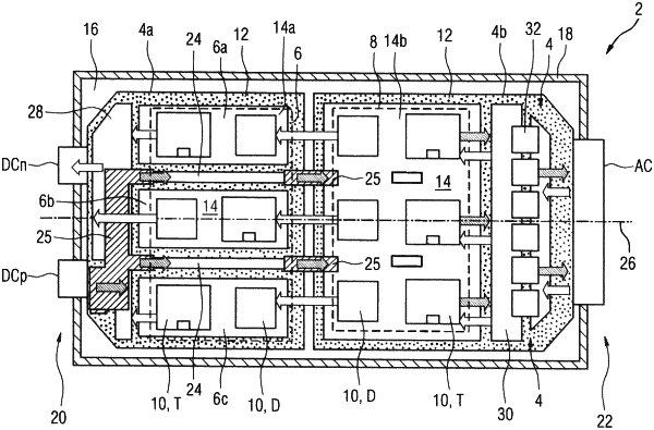
1. A power module, comprising:
a housing,
a first power connector and a second power connector being arranged on a first side of the housing and at least one other power connector being arranged on an opposing second side of the housing;
a substrate;
at least two power semiconductor arrangements disposed in the housing and in contact with the substrate, each power semiconductor arrangement comprising at least one semiconductor component, wherein a first of the at least two power semiconductor arrangements is arranged between a second of the at least two power semiconductor arrangements and the first and second power connectors; and
first supply lines disposed on the substrate and connecting the second power connector to the second power semiconductor arrangement and bypassing the first power semiconductor arrangement symmetrically along two opposing sides of the first power semiconductor arrangement, and a second supply line disposed between the first supply lines and connecting the first power connector to the first power semiconductor arrangement.
|