| CPC H01Q 13/20 (2013.01) [H01Q 3/247 (2013.01)] | 13 Claims |
|
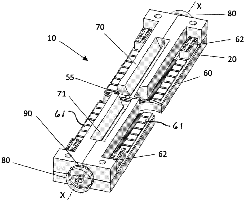
1. An electronically controlled steerable beam antenna, comprising;
a base having a planar surface;
a plurality of semiconductor antenna chips mounted on the planar surface of the base along a longitudinal axis X, each of the antenna chips defining an upper surface;
a ground plane on the upper surface of each of the antenna chips;
an array of semiconductor switches arranged longitudinally in each of the antenna chips, each of the semiconductor switches comprising a ground electrode, a central electrode, and a control electrode, the control electrode being configured for electrical connection to a control circuit;
an array of conductive scattering elements on each of the plurality of antenna chips, wherein each of the conductive scattering elements comprises a first leg connected to the ground plane, a second leg connected to the central electrode of an associated one of the semiconductor switches, and a main portion extending between the first leg and the second leg, wherein at least the main portion is surrounded by air;
a metal spacer disposed on the ground plane, wherein the spacer extends laterally along the ground plane; and
a linear dielectric element mounted on the spacer and the plurality of antenna chips along the longitudinal axis X above the conductive scattering elements, and spaced by an air gap from the conductive scattering elements.
|